I am currently working as a Postgraduate Researcher at the University of Leeds, where I am actively involved in research activities. Prior to this, I successfully completed my master's degree through the renowned Erasmus Mundus joint program, specializing in Tribology and Bachelor's degree in Mechanical Engineering from VTU in Belgaum, India. Further I handle the social media pages for Tribonet and I have my youtube channel Tribo Geek.
Scanning Electron Microscope
13.10.2022
Table of Contents
Introduction
The optical microscopes that use light as the main source to observe any material surface are limited by their resolution in comparison to the electron microscopes. Scanning electron microscopes (SEM) have been commercialized for about 40 years; since then the SEM has been developed for various applications. SEM is used in the fields which deal with observing the features of the specimens in the micro and nano-sized particles. The Fig-1 shows the SEM instrument by Hitachi.
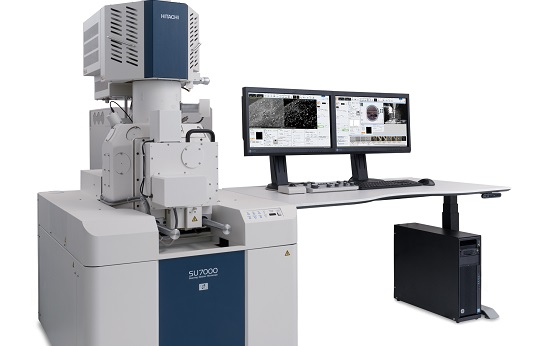
Fig-1 SEM instrument by Hitachi [1]
Definition
SEM is an advanced electron microscope that is used to observe the specimens by irradiating the fine beam of high-energy electrons on the specimens. The variety of signals that are emitted from the surface of the specimen reveals information about the specimen. Information such as external morphology, chemical composition, and crystalline structure of the specimens can be obtained from this technology. The data that is collected from the surface of the specimen is generated as the 2dimensional image which describes the spatial variations in the surface properties of the specimen. The schematic representation of SEM is shown in Fig-2.
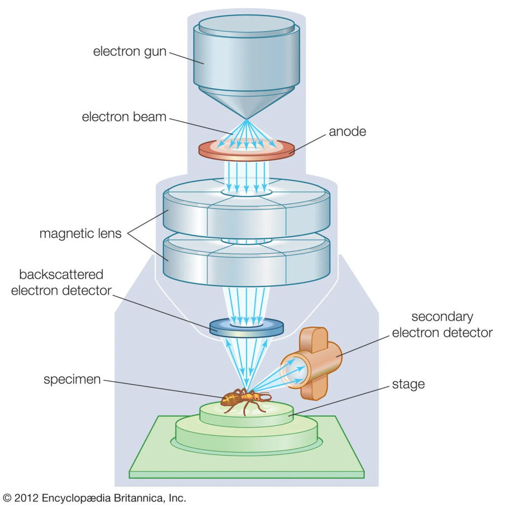

Fig-2 Schematic image of SEM [2]
The basic principle of SEM
SEM technology works on the principle of impinging the fine beam of high-energy electrons on the surface of the specimen and obtaining a variety of signals from the specimen surface to determine its properties. The accelerated electrons in SEM carry a large amount of kinetic energy when focused on the specimen surface. This energy, when impinges on the surface dissipates a variety of signals due to electron-specimen interaction. The combination of signals includes secondary electrons, backscattered electrons, diffracted backscattered electrons, photons, visible light, and heat. These signals are used to determine different information about the specimen surface and in the case of SEM, the secondary electrons and backscattered electrons are mostly used in producing the image of the specimens. Secondary electrons mainly produce the morphology and topographical information whereas backscattered electrons are used to determine the contrasts in the composition of multiphase samples. The schematic representation of the working mechanism of the SEM is shown in the Fig-3.
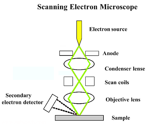
Fig-3 Schematic image of SEM working principle [3]
SEM Instrumentation
SEM is a very complex structure with a variety of components operating in it to analyze the data of the specimen surface. The essential components in the SEM constitute an electron gun, condenser and objective lens, specimen stage, secondary electron detector, image display, recording, and vacuum system.
- Electron gun: The electron gun is used to produce the electron beam that mostly uses thermionic emission from the cathode source (tungsten filament). The filament is heated to a very high temperature (2800K) and the emitted thermoelectric is focused through a metal plate which acts like an anode. This is done in order to focus the current of the electron beam at the desired point.
- Condenser and objective lens: These lenses are used to enable the adjustment of the diameter of the electron beam. A condenser lens helps in strengthening the electron beam and adjusting the diameter of the electron beam when it passes through this lens. An objective lens is used to focus the electron beam onto the specimen surface and it determines the final diameter of the electron beam.
- Specimen stage: This acts as the supporting base of the specimen which stably supports the specimen by moving smoothly in vertical, horizontal, and rotational ways.
- Secondary electron detector: This is used to detect the secondary electrons emitted from the specimens and it is placed above the objective lens. Magnetic fields are utilized in detecting secondary electrons.
- Image display and recording: The output signals obtained from the secondary electron detector are amplified and sent to the display unit. Initially, cathode ray tubes were used for the display units however now the liquid crystal display is being used. Recording of these images is obtained in digital format.
- Vacuum system: The electron optical system and the specimen chamber should be in vacuum conditions and hence the components are evacuated by diffusion pumps. In the case of an oil-free environment then, turbo molecular pumps are used.
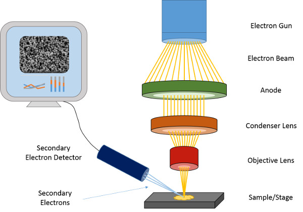

Fig-4 Schematic image of SEM components [4]
Advantages and disadvantages
The image processing and data analysis of the topographical characteristics of any material specimen is very easy in the case of SEM. Using different techniques such as the backscattered electron beam technique, and diffracted backscattered electron techniques then various information such as crystal structure orientation and chemical compositions of the specimens can be obtained. SEM is one of the most used techniques in material surface analysis.
The disadvantages of the SEM include the sizing of the specimen which should be fitted inside the specimen chamber. The specimen compositions also play an important role where the specimens which oxidize at low pressure or the specimens that are wet such as organic materials cannot be determined in this technique. Also, the materials should be electrically conductive or conductive coatings in order to analyze the data.
Application of SEM
The application of SEM is in various fields, it is used to determine high-resolution images of the material’s shapes and determine the chemical compositions by acquiring the elemental maps. SEM is used in identifying the phases based on qualitative chemical analysis or by crystalline structure. Backscattered electron images can be used to determine the discrimination of phases in multiphase specimens. Whereas diffracted backscattered electron detectors are used to determine the micro fabric and crystallographic orientation in specimens.
Reference
[1] https://analyticalscience.wiley.com/do/10.1002/imaging.6389
[2] https://www.britannica.com/technology/scanning-electron-microscope
[3]https://www.thermofisher.com/blog/materials/what-is-sem-scanning-electron-microscopy-explained/
[4] https://www.jove.com/v/5656/scanning-electron-microscopy-sem
Leave a Reply
You must be logged in to post a comment.
Good